The 2nm GAA process offers a significant performance and efficiency boost over Samsung’s older manufacturing processes, but the company’s Foundry Vice President says that shrinking the nodes only offers minor benefits and believes that there is a requirement to explore other alternatives. For this purpose, the Korean technology behemoth has proposed a ‘Design and Process Integration Optimization’ (DTCO) method, which researches modifications that can be applied to bolster the prowess of cutting-edge nodes.
One area that Samsung has improved upon is transitioning from FinFET to GAA structures, maximizing current control capabilities, and allowing for its 2nm node to introduce a significant number of improvements
Speaking at the eighth Semiconductor Industry-Academia-Research Exchange Workshop held at COEX in Samseong-dong, Seoul, Samsung Electronics Foundry Vice President Shin Jong-shin says that the industry has shifted towards DTCO, with both the company and its rival TSMC having dedicated teams pursuing both design and process improvements.
“Now, process miniaturization alone can only lead to improvements of 10-15%. As process performance improvement reaches its limits, the industry is paying attention to DTCO. At 7nm, approximately 10% of the overall performance improvement is due to DTCO. We expect that share to reach 50% at 3nm and below. Both Samsung and TSMC have dedicated DTCO teams and are pursuing simultaneous design and process improvements.”
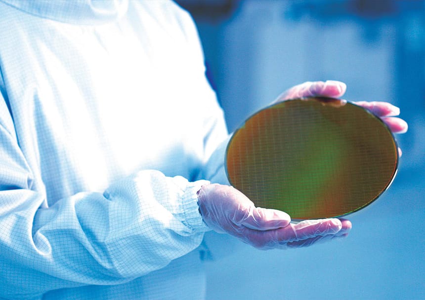
According to The Elec, at DTCO, engineers review existing process constraints while exploring alternatives based on designer requests, such as Tesla. By modifying these processes, cells can be placed more efficiently, and surface area can be reduced. Samsung has already employed the FinFET architecture in previous iterations and has moved to Gate-All-Around (GAA) structures, starting with its 3nm variant, which did not produce adequate yields, but the 2nm node is showing a ton of promise.
“When going from N node to M node, the performance improvement is about 15%, and the area reduction is also about 15%. Unlike the artificial intelligence (AI) field where performance doubles every few months, in the world of semiconductor processing, even a 1-2% difference is very important. A 1-2% performance difference can become a criterion for process selection.”
In addition to exploring other alternatives, Samsung is leveraging AI in an attempt to automatically create new cell structures that can achieve a smaller area and reduce power consumption. Samsung Electronics Foundry executive says that DTCO will further expand into developing System-Process Co-Optimization (SPCO) and System-Design-Process Co-Optimization (SDTCO), which should further refine this process.
Samsung is reported to have completed the basic design of its second-generation 2nm GAA process, with its third iteration SF2P+ estimated to be implemented within two years. It is possible that the Korean foundry has ventured deep into DTCO to develop improved variations of its 2nm GAA process, which is why it might have delayed its 1.4nm node in favor of improving the current process rather than competing head-on with TSMC.
News Source: The Elec
Follow Wccftech on Google or add us as a preferred source, to get our news coverage and reviews in your feeds.
