The high tool allows processing of structures to sub-5 nm which can be achieved in thick resist – up to 10 micrometres (μm) – with almost vertical sidewalls.
Using the higher kV setting, the machine’s can use can be extended beyond lithography to electron displacement.
The system creates new opportunities for fine-geometry capability in novel device fabrication, across electronics, photonics, and bio-nano technology. It is available for collaborative research.
The facility is supported by a grant from the Engineering and Physical Sciences Research Council (EPSRC).
The university has developed lithography processes for a number resist types. It uses Genisys software to carry out pattern optimisation. It has dedicated spin coaters and hotplates for electron beam resist coating processes.
The EBL tools are integrated with a scanning electron microscope (SEM), the JEOL IT-800i. This is optimised for semiconductor materials and fabrication characterisation purposes. The facility can also provide “mix and match” lithography, in conjunction with the deep-ultraviolet scanner.
In late 2024, the facility will receive a second EBL tool, the JEOL JBX-A9, a high-volume 300 mm wafer, 100kV tool. This will also be the first of its type outside of Japan.
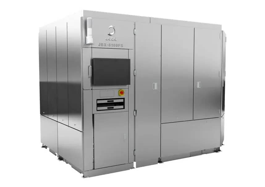
EBL system – JEOL JBX-8100FS G3
- operating at 100kV and 200kV
- current range 100 picoamperes to 200 nanoamperes
- up to 200 megahertz scan speed
- substrate sizes up to 200mm
- minimum feature size <10nm
- 12 cassette autoloader
- 1.6nm minimum spot size (at 100kV)
- high throughput mode: +/-20nm overlay and stitching accuracy; data increment 0.5μm
- high resolution mode: +/-9nm overlay stitching accuracy; data increment 0.05μm
- field size: 1x1mm at 100kV; 0.5 x 0.5mm at 200kV
