Swansea University in Wales has installed gallium tri-oxide (Ga2O3) deposition equipment at its Centre for Integrated Semiconductor Materials (CISM).
In the correct crystal form, Ga2O3 is an ultra-wide bandgap semiconductor (~4.8eV), suiting it to high voltage semiconductors. The semiconductor can also be used in ultra-violet detectors.
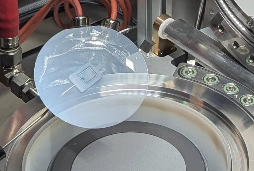
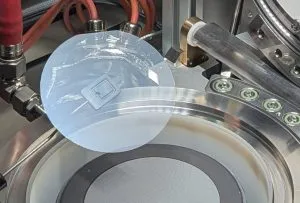
CISM has an MOCVD (metal-organic chemical vapour deposition) laboratory built around Aixtron equipment, to which it has added a close-coupled shower head deposition system allowing it to grow crystalline gallium oxide thin films on 4 inch (100mm) substrates “which have been tested and shown to be very uniform and of extremely high quality”, according to the university.
“This new facility represents a major step forward for our research,” said Swansea MOCVD research head Dan Lamb. “With this equipment, we can push the boundaries of our existing work while also creating new opportunities for collaboration with research groups across the UK, and beyond.”
“Swansea University’s MOCVD capability is now accessible. “Researchers can gain access to feasibility studies through Swansea partnering with the UK National Epitaxy Facility’s pump-priming scheme,” said Professor John Heffernan of the UK National Epitaxy Facility – which supports semiconductor research in UK universities.
Swansea is part of the South Wales compound semiconductor cluster, branded ‘CSconnected’, which includes centres owned by Vishay, KLA, Microchip and IQE.
“The [gallium oxide] achievement is timely given the recent announcement of a £250m silicon carbide investment by Vishay supported by the UK Government’s Automotive Transformation Fund in it’s Newport plant to expand advanced wide band gap power semiconductor component manufacturing”, said the university.
The UK’s EPSRC (Engineering and Physical Sciences Research Council) provided a £2.7m grant towards the MOCVD equipment at the Swansea lab.
Photo: 4 inch Ga2O3-on-sapphire wafer unloading from the Aixtron close-coupled shower head at Swansea University’s Oxide and Chalcogenide MOCVD lab.
