It is working towards a new generation of AI-enabled sensors that can record the scene, perceive its content and act upon the understanding.
“The communication between the different tiers requires advanced interconnection technologies, a requirement that hybrid bonding meets because of its very fine pitch in the micrometer, and even sub-micrometer, range,” said Leti scientist Renan Bouis. “High-density through-silicon via has a density that enables signal transmission through the middle tiers. Both technologies contribute to the reduction of wire length, a critical factor in enhancing the performance of 3D-stacked architectures.”
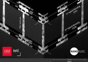
A three-layer proof-of-concept has been produced, featuring two embedded Cu-Cu hybrid-bonding interfaces, one face-to-face and the other face-to-back, with one of the wafers pierced with high-density TSVs.
“This sets the stage to work on demonstrating a fully functional three-layer, smart CMOS image sensor, with edge AI capable of addressing high performance semantic segmentation and object-detection applications,” said project manager Eric Ollier.
Last year at ECTC, the lab reported a two-layer stack with 10μm high 1μm diameter TSV and face-to-back hybrid bonding. The vias for a two-layer stack are now 6μm high.
“Our 1-by-6μm copper TSV offer improved electrical resistance and isolation performance compared to our 1-by-10μm TSV, thanks to optimised thinning that enabled us to reduce the substrate thickness with good uniformity,” said fellow scientist Stéphan Borel. “This reduced height led to a 40% decrease in electrical resistance, in proportion with the length reduction. Simultaneous lowering of the aspect ratio increased the step coverage of the isolation liner, leading to a better voltage withstand.”
The relevant ECTC 2024 papers are:
‘Backside thinning process development for high-density TSV in a 3-layer integration’.
‘3-layer fine pitch Cu-Cu hybrid bonding demonstrator with high density TSV For advanced CMOS image sensor applications’
‘Low resistance and high isolation HD TSV for 3-layer CMOS image sensors’


